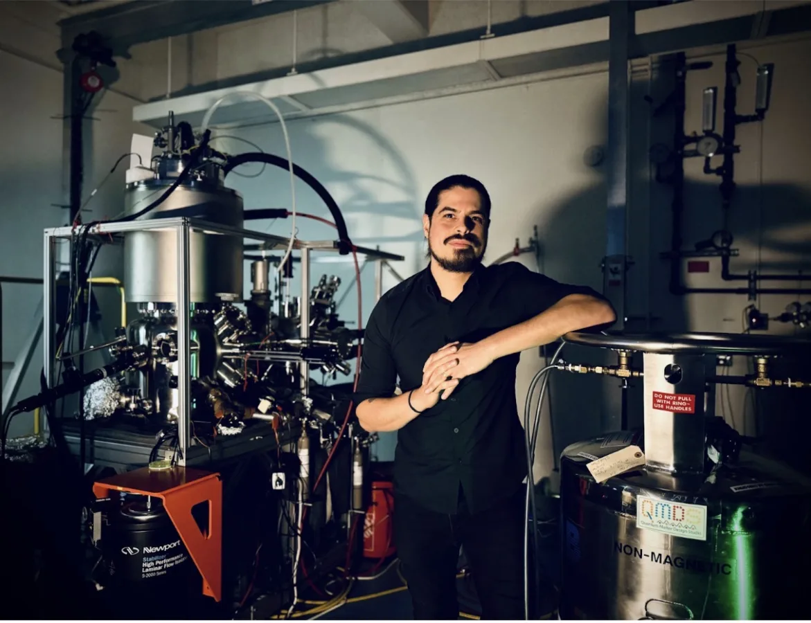
UCLA Assistant Professor of Physics and Astronomy Christopher Gutiérrez has been awarded a prestigious Early Career Research Program grant from the Department of Energy (DOE) Office of Basic Energy Sciences. The award, $875,000 over five years, will support research on uncovering the atomic-scale nature of current-flow in exotic quantum materials, knowledge that could help advance future energy efficient technologies and deepen our understanding of a phase of matter called a charge density wave.
The project harnesses a technique called scanning tunneling microscopy (STM) to image electrons with sub-atomic resolution. “Our microscope images atomic surfaces similarly to how a finger reads Braille,” Gutiérrez explains. “But instead of touching the surface, we hover just a few atomic distances above it and detect an incredibly tiny quantum tunnel current—about a million millionth (10-12) the electrical current in a kitchen refrigerator.”
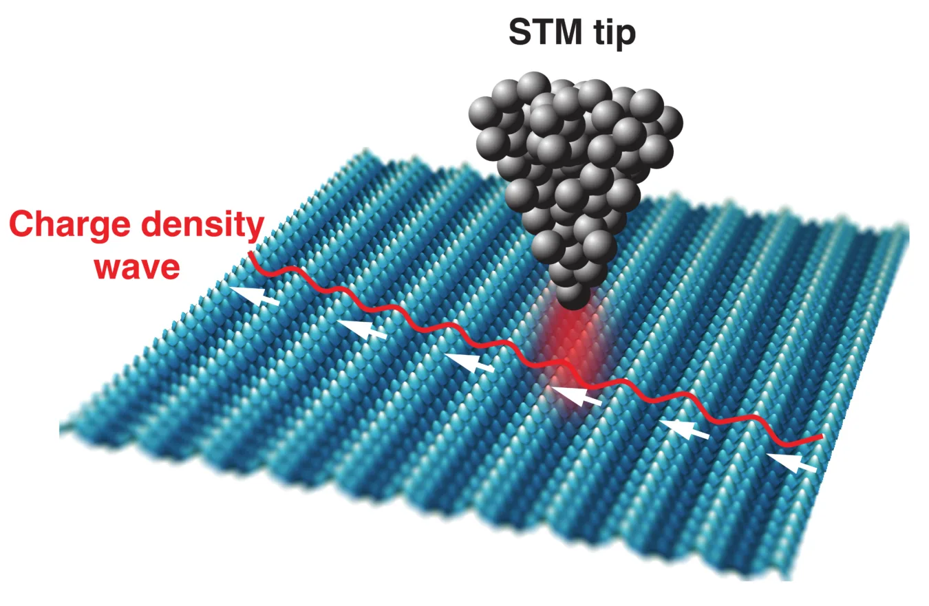
Cartoon diagram of a new method, current tuned scanning tunneling microscopy (CT-STM), to visualize the sliding of a charge density wave. (Photo Credit: Christopher Gutiérrez)
Gutiérrez’s Early Career project focuses on a phase of matter called a charge density wave, in which electrons and lattice atoms spontaneously organize into a periodic pattern distinct from the original crystal structure. Though scientists have studied this phase for decades, how these waves actually move—or slide—across a material at the atomic scale remains poorly understood. Since charge density waves appear in a wide range of materials, including high-temperature superconductors, deciphering their motion is of great interest.
“Charge density waves behave a bit like a block on a ramp,” explains Gutiérrez. “At low voltages, imperfections in the crystal initially pin them in place, like friction holding the block still. But increase the voltage, or tilt the ramp, and the charge density wave can break free and slide. Although we have many theories on how this de-pinning occurs, the process has never been recorded directly.”
To investigate this, Gutiérrez and his group, the Quantum Matter Design Studio, is developing a new technique called current tuned STM (CT-STM), which combines atomic imaging with simultaneous electronic transport measurements. Driving a current through the material causes the charge density wave to distort and move, which they can visualize using the STM tip. “It’s like turning a static Braille surface into a dynamic display,” he explains.
Building on their CT-STM work at UCLA, Gutiérrez’s team has secured highly competitive access to world-class synchrotron resources at the Advanced Light Source, a Department of Energy scientific user facility at Lawrence Berkeley National Laboratory, where they will conduct novel current tuned photoemission measurements on charge density wave materials.
UCLA has a rich history in charge density wave research stretching back decades. Gutiérrez himself first encountered the topic as a UCLA undergraduate in a course taught by Distinguished Professor and current Department Chair Stuart Brown, a charge density wave expert and collaborator. Prof. Gutiérrez now teaches that same course where charge density waves are once again brought into the classroom.
“It’s an amazing full-circle moment,” says Gutiérrez. “Returning to my hometown and UCLA as a faculty member and leading my own research group to continue this work is incredibly exciting.”
This generous DOE support will directly fund the hands-on training of undergraduates, Ph.D. students, and postdoctoral scholars. Like Gutiérrez once did, these trainees represent the next-generation of scientists who will work at the forefront of quantum materials research. “By engaging with cutting-edge technology and tackling complex scientific challenges, they will gain valuable skills in experimental physics, data analysis, and critical problem-solving, which will prepare them for leading careers in either academia or high-tech industries,” said Gutiérrez.